Informasi penting
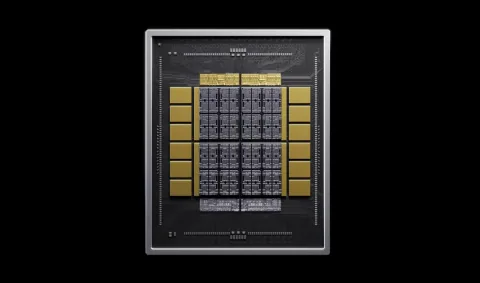
Samsung is reportedly entering a partnership with TSMC to supply base dies for NVIDIA's NVHBM memory standard. This new architecture incorporates the controller directly into the 3D HBM stack to improve overall system performance.
NVIDIA mandates that the base die for NVHBM must be manufactured using TSMC's 3 nm node due to IP optimization requirements. Consequently, Samsung will utilize TSMC for these specific components while continuing to manufacture the memory portion using its own sixth-generation 10 nm processes.
The NVHBM standard promises significant technical improvements over HBM4E, including a 30% increase in memory bandwidth and a 15% reduction in power consumption. Additionally, the design allows for 25% more usable compute die area on the processing unit.
These efficiency gains provide extra thermal headroom for compute dies. With the projected bandwidth improvements, a single NVHBM unit could potentially reach speeds of approximately 5.2 TB/s, reflecting a shift toward more powerful memory alternatives.